Novel GaAs plasmonic terahertz detector: recent discovery expands capabilities for the frequency response optimization
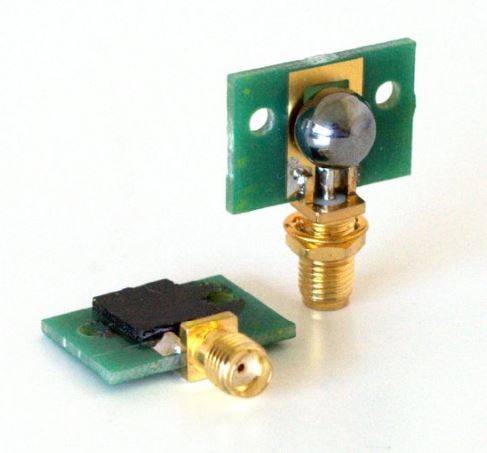 TERASENSE can proudly claim to have a truly revolutionary technology for terahertz imaging, which is quite unusual in certain respects and has nothing to do with either semiconducting bolometers or heterodyne detectors. Our technology is based on GaAs semiconductors used for making pixels, while our pixels themselves represent high-speed plasmonic terahertz detectors that unlike some others types of sensor are capable of operating at room temperatures.
Of course, as in any other field, there are no boundaries to knowledge in THz imaging technology and there are a lot more to be discovered . Having a state-of-the-art research lab at their disposal TERASENSE scientists have been continuously working to learn more about their products and have recently made another breakthrough as described below.
 Many of our customers already know that our terahertz detectors employed in our THz sensor arrays /imaging cameras are of broad-band type, which enables them to pick up radiation within our whole certified range of 50 GHz – 700 GHz. However, the sensitivity (i.e. the measured frequency response) of our detectors is not monotonic and therefore does not represent a continuous curve. Due to radiation interference within the of detector’s detector’s substrate (i.e. crystal inside), its responsivity consists of multiple peaks and drops. We new that and always told our customers that our specialists can tune positions of the maximums in responsivity curve at manufacturing stage to match with frequencies preferred by our Client.
In addition to and based on that, a group of investigative young scientists including Anton Shchepetilnikov, Gombo Tsydynzhapov, Viacheslav Muravev, Pavel Gusikhin, Alexey Dremin, Yuriy Nefyodov, B. Kaysin - all with PhD degree in solid state physics - lead by Prof. Dr. Igor Kukushkin recently conducted a research project aimed at deeper exploring the oscillatory behavior of our single-pixel GaAs plasmonic THz detectors over a wide range of sub-THz frequencies. As a result they established a clear dependence between the substrate thickness of THz detectors and the actual frequency response and sensitivity maximums that can be reached at certain frequencies.
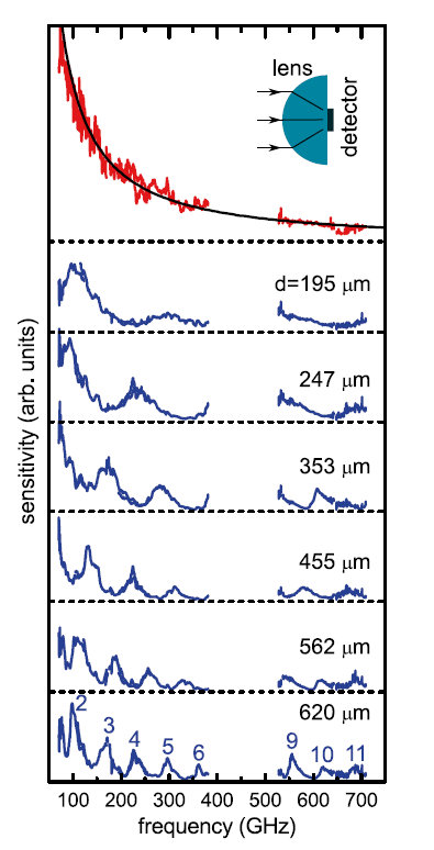
Their study revealed that such frequency dependence caused by the interference of electromagnetic waves inside the detector substrate can be effectively used for optimizing the desired operating frequency simply by adjusting the substrate thickness. It applies to both our single-pixel (point ) THz detectors as discrete elements and our sensor arrays/THz imaging cameras (as a set of point detectors). The picture posted here shows a few key diagrams of frequency response as a function of substrate thickness.
Moreover, their study shows that a hemispherical silicon lens mounted on such single-pixel THz detector can effectively suppress interference within the substrate and, consequently, which may help us achieve a more even and predictable frequency response.
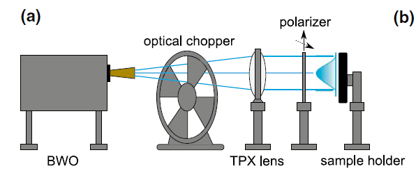 The picture below shows the elements of experimental setup used for measuring the frequency response of our point THz detector. We employed a few BWO sources to generate a CW test signal over the frequency ranges of 65 GHz–384 GHz and 530– 710 GHz. The frequency span between 384 GHz – 530 GHz was not checked simply due to lack of respective CW sources at hand, but our researchers believe that our THz detectors remains sensitive in that domain too. You are welcome to take a close look at our findings in the article Optimization of the frequency response of a novel GaAs plasmonic terahertz detector (A. V. Shchepetilnikov et al.) posted online 12 November 2019 in Springer Science, part of Springer Nature 2019.
(Optical and Quantum Electronics (2019) 51:376 https://doi.org/10.1007/s11082-019-2093-4)
The practical implications of this discovery can hardly be overestimated as it will help improve THz imaging technique for such application fields as real-time THz imaging in industrial NDT and security screening and telecommunications. As our technology employs standard processes widely used in semiconductor manufacturing for mass-market production, it allows us to claim a reasonable price and ensure high-performance and fast response rate. There is no doubt that the achievement made by our scientists will help us better meet the customers’ needs and wants in the future and will streamline the development process of our products.