TeraSense technology

TeraSense has developed an original patent-protected technology for making a new generation of semiconductor detector arrays for terahertz imaging. The detectors developed by TeraSense have high sensitivity compared to other available detectors working in the THz range (0.1 — 0.7) THz. TeraSense detectors have an advantage with their low cost and ease of fabrication in large quantities in the form of 2D arrays, thanks to compatibility of the TeraSense technology with mass-production lines of semiconductor industry. The detector arrays are scalable in the number of pixels.
TeraSense imaging chips enable to produce an extremely compact and sensitive THz camera. It is essential that the spatial resolution of such a camera is around 1 mm and its registration time is less than 1 second. This makes it possible to effectively use TeraSense imaging chips for medical diagnostics, non-destructive testing and many other terahertz applications.

")
For the terahertz generation purposes TeraSense uses proprietary IMPATT and backward-wave oscillator (BWO) technologies. These THz sources allow delivery of up to 1 W power at sub-THz frequencies (0.1 — 0.3) THz.
TeraSense patents
Apparatus and method of detecting electromagnetic radiation (US 8772890 B2)
The high speed and miniature detection system, especially for electromagnetic radiation in the GHz and THz range comprises a semiconductor structure having a 2D charge carrier layer or a quasi 2D charge carrier layer with incorporated single or multiple defects, at least first and second contacts to the charge carrier layer, and a device for measuring photovoltage between the first and second contacts. System operation in various embodiments relies on resonant excitation of plasma waves in the semiconductor structure.
Tera- and gigahertz solid state miniature spectrometer (US 8159667 B2)
The high speed miniature tera- and gigahertz electromagnetic radiation on-chip spectrometer that comprises a tunable solid state 2D charge carrier layer or a quasi 2D charge carrier layer with incorporated single or multiple defects, at least first and second contacts to the charge carrier layer. The device also includes an apparatus for measuring the device response between the first and second contacts, and an apparatus for controllable tuning of at least one of the charge carrier layer parameters. The operation principle is based on the fact that radiation of different wavelengths excites distinct sets of plasma modes in the charge carrier layer.
High-speed giga-terahertz imaging device and method (US 20130161514 A1)
The high-speed room-temperature imaging system, especially for electromagnetic radiation in the GHz and THz frequency range, is based on the sensor consisting of a matrix of plasmonic semiconductor detectors. The imaging system comprises a radiation source module, a terahertz beam director module, a plasmonic imaging sensor module, and a signal processing module. The entire image is formed immediately ensuring high-speed image acquisition. Images can be acquired either at a single frequency (discrete spectrum) or wide frequency bands (continuous spectrum). The imaging system can be used in defectoscopy, inspection, medical and other applications.
Scientific concepts
TeraSense technology is a spin off from long-term fundamental research carried out in the field of plasmonics showing a surge of research during the last few decades. An important impetus comes from the physical property of plasma waves to confine electromagnetic radiation at sub-wavelength scales. Furthermore, plasma waves may be efficiently manipulated on a chip. The plasmonics concept has already found a wealth of applications for devices working in the optical part of the spectrum. However, recent progress in the purity of semiconductor AlGaAs/GaAs nanostructures has made it possible to adapt the plasmonic concepts from the optical region of the spectrum to the microwave and terahertz (THz) bands.
Related publications
Surface plasmon subwavelength optics
W.L. Barnes, A. Dereux, T.W. Ebbesen
Nature 424, 824 (2003).
Unfortunately, standard two-dimensional (2D) plasmons are observable only when their frequency ω >1/τ, where the momentum relaxation time τ essentially decreases with increasing temperature. Hence, the plasmonic effects are visible only at sufficiently large frequencies and sufficiently low temperatures. Indeed, 2D plasma waves at frequencies attractive for applications with f < 500 GHz have been observed only at cryogenic temperatures T< 80 K. This fact severely impedes the advancement of terahertz applications for plasmonic electronics.
Related publications
 | Measurement of Magneto-Plasma Excitation Relaxation Time in the Two-Dimensional Electron System I.V. Andreev, V.M. Muravev, V.N. Belyanin, and I. V. Kukushkin |
| | V.M. Muravev, I.V. Kukushkin |
One way to circumvent this imposed limitation is to deal with relativistic plasma excitations — the novel type of plasma waves discovered recently in a gated 2D electron system. These weakly damped plasma waves are excited in high-conductivity 2 πσ > c electron system and exhibit a strong polaritonic nature. It was proved that such relativistic plasmons survive up to room temperature in the microwave and sub-THz frequency ranges.
Related publications
| Novel Relativistic Plasma Excitations in a Gated Two-Dimensional Electron System V.M. Muravev, P A. Gusikhin, I.V. Andreev, and I.V. Kukushkin |
| Observation of Plasma Waves with Anomalously Weak Damping in a Two-Dimensional Electron System P.A. Gusikhin, V.M. Muravev, and I.V. Kukushkin |
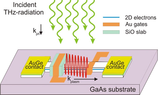
In the TeraSense detector, terahertz radiation is converted into the alternating potential of a relativistic plasma wave via a broadband antenna structure deposited onto the crystal surface. Moreover, the alternating potential of the plasma wave is rectified to yield the measured photoresponse signal owing to the asymmetry of the plasmonic waveguide. The geometry of the detector can be chosen to match a specific THz frequency band.
TeraSense semiconductor fab
Terasense imaging chip production consists of several lithographic steps conducted in special clean room conditions of TeraSense semiconductor fab. A clean room is an environment that has a low level of environmental pollutants such as dust, airborne microbes and chemical vapors. It also has a controlled level of contamination that is specified by the number of size-defined particles per cubic meter. TeraSense facilities have class 1000 (ISO 6) cleanroom conditions in the walking area and 100 (ISO 5) conditions under the equipment.
For patterning of GaAs wafers TeraSense has a special production line. The supporting infrastructure consists of a water purification system, a pure gas installation, a photo-resist spinner, a wet bench, an UV-exposure system, a metal deposition system, an inspection microscope, a photo-resist ashing system, and an ion etching system. Electron beam lithography is used to achieve and inspect structures at sizes below one micrometer. Electron beam lithography uses a finely focused electron beam for exposure of resist material.
 |  |
 |  |
TeraSense perspectives
TeraSense has a strong team of 40 skilled scientists and engineers, all possessing a PhD in the field of microwave and terahertz technology. The team is constantly working on improving the sensitivity of TeraSense terahertz detectors. Our unique research and development capabilities allow forecasting a substantial increase in sensitivity in the next few years.
We plan to switch from expensive GaAs technology to a widespread and cheap Si technology. This step will enable us to integrate THz detection and amplification circuits on the same chip. The latter will increase the number of pixels and simplify production of TeraSense chips and devices.
Commercialization of Terasense technologies could lead to creation of a new mass market of terahertz devices. We are actively working on the first industrial applications of THz waves in various areas: medicine, quality control, and security.
Current development rates of terahertz imaging and detection systems suggest that within a mid-term perspective (2020 – 2025) THz systems will be successfully integrated into the majority of production lines and process cycles. By various estimates at this stage the market size of terahertz devices is expected to reach (7–9) B$ per year.
Related info
Terahertz Components & Systems: Technology and Market trends UPDATE 2016
Report by Tematys In 2013,
Tematys has released a Terahertz studies report on market and technology trends covering the electromagnetic spectrum from 200 GHz to 10 THz.