Gunn diodes
The Gunn diode (or transferred electron devices, TED) is a semiconductor component with negative resistance that converts the energy of a constant-voltage power source into the energy of high-frequency oscillations due to the formation of a strong field region (domain). Despite the fact that this electronic component is referred to as a «diode», this technology does not rely on PN junctions or the Avalanche Principle; it is composed only of N-doped semiconductor material.
In 1963, while investigating the properties of semiconducting compounds in the high electric field, J. Gunn discovered the spontaneous appearance of electric field oscillations in homogeneous samples of gallium arsenide and indium phosphide, if the applied electric field strength is larger than a certain threshold. This effect was called the Gunn Effect after its discoverer, while microwave generators based on it are called Gunn diode generators. Gunn’s discovery concluded an extended period of research efforts towards finding phenomena providing negative bulk conductance in solids.
Principle of operation
Material and structure
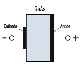
The Gunn diode (GD) is a homogeneous semiconducting crystal based on III-V group elements, including GaAs, InSb, InAs, ZnSe, and CdTe. However, the most common and the most studied material used for Gunn diodes is GaAs. Figure 1 shows the schematic structure of the Gunn diode.
Gallium arsenide is a two-valley semiconductor. Figure 2 displays the zone structure of GaAs.
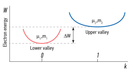
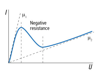
If the applied electric field is large enough, part of the electrons acquire energy comparable to the inter-valley transition energy ΔW, and they pass from the lower valley to the upper one. The large electron-mobility difference between the two bands leads to the fact that, starting from the critical value of the electric filed (Eth), the average electron drift velocity (Vd) decreases with increasing the electric field. If the electric field is larger than the threshold value (Eth), the volt-ampere characteristics of the GD includes the negative differential resistance area (see Figure 3).
Formation of strong field domains
In the negative differential resistance area the homogeneous charge and field distribution in the bulk of the semiconductor are unstable, involving the possibility of domain formation.
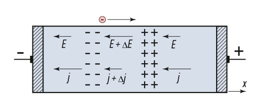
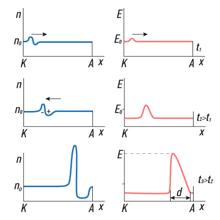
The Gunn Effect is related to the fact that a region of a strong electric field called an electric domain periodically arises, moves, and disappears in the sample. The domain arises because the homogeneous electric field distribution is unstable at a negative differential resistance. Suppose that an inhomogeneous electron distribution accidentally occures in the form of a dipole layer in the semiconductor—the electron concentration increases in one region and decreases in the other (Figure 4). An additional field (ΔE) arises between these charged regions(as between the plates of a charged capacitor). If it is added to the external field (E), and the differential resistance of the sample is positive (i.e., the current increases with increasing field E), then the current inside the layer is greater than outside (Δj>0). Therefore, electrons flow out of the region with increased density in a larger quantity than those flowing inside. Consequently, the inhomogeneity dissolves. If, however, the differential resistance is negative (the current decreases with increasing field), the current density is less in the region of the larger field (i.e., inside the layer). The originally emerging inhomogeneity does not dissolve; on the contrary, it increases. The voltage drop on the dipole layer also increases and falls outside it (since the total voltage on the sample is set). Eventually, an electric domain is formed (Figure 5).
Since the domain is formed by current carriers—”free”-conducting electrons—it moves in their drift direction with a velocity (v) close to the drift velocity of the carriers outside the domain. Usually, the domain arises at the cathode and not inside the sample. The domain disappears, having reached the anode. As the domain disappears, the voltage drop on it decreases and, accordingly, increases on the rest of the sample. At the same time, the current in the sample increases since the field outside the domain increases; as this field approaches the threshold field (Eth), the current density approaches the maximum value. When the field outside the domain exceeds the threshold, a new domain begins to form at the cathode, the current falls, and the process repeats. The frequency (ν) of the current oscillations is equal to the reciprocal of the domain passage time through the sample: ν=v/l.
Work regimes
The most studied and most commonly used work regime is the domain regime of generators based on the Gunn diode. These regimes are characterized by the existence of the dipole domain formed during most of the oscillation period.
In the limiting accumulation of the bulk charge regime (LABC), the voltage frequency is so large that the voltage drop on the GD passes the negative differential resistance area faster compared to τ. The domain has no sufficient time to form, and the dynamical volt-ampere characteristics coincide with the characteristics of the drift speed, Vd (E).
Other regimes between the LABC regime and the domain regime are called hybrid regimes. In these regimes, τ is comparable to the oscillation period, and during part of it, there exists a non-equilibrium spatial distribution of the charge in the sample. These regimes are typical for GDs with f ≥ 8…10GHz.
Equivalent scheme
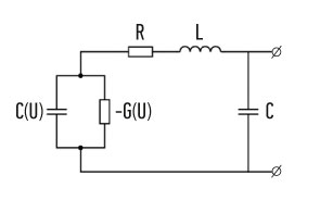
The simplified scheme of the active layer of the GD is shown in Figure 6, where the active area of the diode is modeled by the parallelly connected non-linear capacitance, C (U), which reflects the charge accumulation process, and negative conductance G (U). Both values of G and C depend on the constant voltage as well as on the microwave voltage amplitude (Um) and frequency.
